<--- Back to Details
First PageDocument Content
Materials science / Projectors / Electromagnetism / Semiconductor devices / Transducers / Digital micromirror device / Micromirror device / Digital Light Processing / Microelectromechanical systems / Microtechnology / Optoelectronics / Technology
Date: 2006-01-20 16:34:37
Materials science
Projectors
Electromagnetism
Semiconductor devices
Transducers
Digital micromirror device
Micromirror device
Digital Light Processing
Microelectromechanical systems
Microtechnology
Optoelectronics
Technology

Digital Light Processing and MEMS: Timely Convergence for a Bright Future Larry J. Hornbeck Texas Instruments Inc. Dallas, Texas Keywords: Digital Micromirror Device™, DMD™, Digital Light Processing™, DLP™, spati
Add to Reading List

Source URL: focus.ti.com

Download Document from Source Website

File Size: 1,42 MB

Share Document on Facebook

Similar Documents

Quantum Communications using Semiconductor Devices Andrew Shields Toshiba Research Europe Ltd 208 Science Park, Milton Road, Cambridge CB40GZ. UK www.quantum.toshiba.co.uk *

Quantum Communications using Semiconductor Devices Andrew Shields Toshiba Research Europe Ltd 208 Science Park, Milton Road, Cambridge CB40GZ. UK www.quantum.toshiba.co.uk *

DocID: 1vqum - View Document

Dear Colleagues: Semiconductor Research Corporation (SRC) Global Research Collaboration (GRC) is soliciting White Papers in the thrust area of Logic and Memory Devices. The white paper, limited to two pages and addressin

Dear Colleagues: Semiconductor Research Corporation (SRC) Global Research Collaboration (GRC) is soliciting White Papers in the thrust area of Logic and Memory Devices. The white paper, limited to two pages and addressin

DocID: 1uNQx - View Document

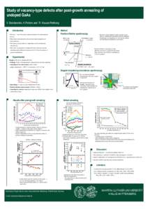
Study of vacancy-type defects after post-growth annealing of undoped GaAs V. Bondarenko, K.Petters and R. Krause-Rehberg Introduction • SI GaAs  one of the most common materials for semiconductor devices

Study of vacancy-type defects after post-growth annealing of undoped GaAs V. Bondarenko, K.Petters and R. Krause-Rehberg Introduction • SI GaAs  one of the most common materials for semiconductor devices

DocID: 1tQeR - View Document

  	
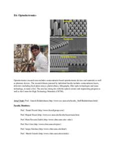
   E6: Optoelectronics  Optoelectronics research area includes semiconductor based optoelectronic devices and materials as well

    E6: Optoelectronics Optoelectronics research area includes semiconductor based optoelectronic devices and materials as well

DocID: 1sFF2 - View Document

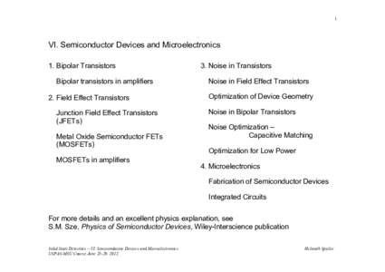
1  VI. Semiconductor Devices and Microelectronics 1. Bipolar Transistors Bipolar transistors in amplifiers 2. Field Effect Transistors

1 VI. Semiconductor Devices and Microelectronics 1. Bipolar Transistors Bipolar transistors in amplifiers 2. Field Effect Transistors

DocID: 1sy2o - View Document