Back to Results
First PageMeta Content
Semiconductor device fabrication / High-temperature superconductors / Coating / Printing / Pulsed laser deposition / Yttrium barium copper oxide / Oak Ridge National Laboratory / Chemistry / Thin film deposition / Materials science


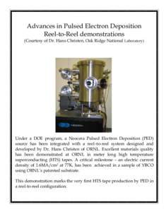
Advances in Pulsed Electron Deposition Reel-to-Reel demonstrations (Courtesy of Dr. Hans Christen, Oak Ridge National Laboratory) Under a DOE program, a Neocera Pulsed Electron Deposition (PED) source has been integrated
Add to Reading List

Document Date: 2013-01-04 14:36:03


Open Document

File Size: 177,94 KB

Share Result on Facebook

City

Beltsville / /

Company

Oak Ridge National Laboratory / Contact Information Neocera Inc / /

Country

United States / /

/

/

IndustryTerm

high volume manufacturing / large scale applications / /

Person

Hans Christen / Pulsed Electron / /

/

ProvinceOrState

Maryland / /

Technology

Laser / PED technology / /

SocialTag