<--- Back to Details
| First Page | Document Content | |
|---|---|---|
 Date: 2014-03-30 21:14:00Extreme ultraviolet lithography Multiple patterning Nanoimprint lithography Immersion lithography Electron beam lithography Maskless lithography Photomask Resist Lithography Microtechnology Materials science Technology |
Add to Reading List |
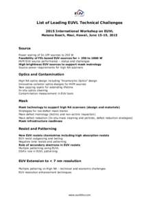 | List of Leading EUVL Technical Challenges 2015 International Workshop on EUVL Makena Beach, Maui, Hawaii, June 15-19, 2015 Source Power scaling of Sn LPP sources to 250 WDocID: 1b2K7 - View Document |
 | Graduate Seminar Design for Manufacturability and Reliability in Extreme Scaling and Beyond ECE Seminar CommitteeDocID: 18osC - View Document |
 | Design Impact of FinFETs Carey Robertson Product Marketing DirectorDocID: 11ySh - View Document |
 | Datasheet Sentaurus Lithography Predictive Modeling of Lithographic Processes OverviewDocID: ZgcH - View Document |
 | At The Edge EM EXPLORER Simulation of Wafer Topography Effects in Double Patterning LithographyDocID: XXN4 - View Document |
 INTERNATIONAL TECHNOLOGY ROADMAP FOR SEMICONDUCTORS[removed]EDITION