<--- Back to Details
| First Page | Document Content | |
|---|---|---|
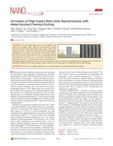 Date: 2011-12-15 14:23:18Chemistry Semiconductor device fabrication Microtechnology Materials science Technology Etching Nanowire Dry etching Gallium arsenide Wafer Chemical milling Photolithography |
Add to Reading List |
 | acs_NL_nl-2011-02708d 1..5DocID: 1qJbN - View Document |
 | Etching mechanism of the single-step through-silicon-via dry etch using SF6/C4F8 chemistry Zihao Ouyang, D. N. Ruzic, Mark Kiehlbauch, Alex Schrinsky, and Kevin Torek Citation: Journal of Vacuum Science & Technology A 32DocID: 1l7f1 - View Document |
 | Wet and Dry Etching Avinash P. Nayak*, Logeeswaran VJ¥ and M. Saif Islamǂ University of California, Davis. California. * ¥ ǂDocID: 1bjfp - View Document |
 | Dry EtchOct2011.qxp:44 AMDocID: 1alXR - View Document |
 | Dry Etch and Plasma System 1. Scope 1.1 This document provides operating procedures and requirements to etch silicon or silica with gas plasma system.DocID: 138iY - View Document |
 acs_NL_nl-2011-02708d 1..5